MCP2518FD click
Product Code: MIKROE-3060


The physical layer is implemented by using a separate IC, which provides increased robustness, required for the automotive applications. It features three operating modes, remote wake-up via the CAN, and offers ideally passive behavior on the CAN bus when it is powered off. These features allow MCP2518FD click to be used for the development of a wide range of automotive diagnostic applications, even on MCUs that do not natively support CAN interface.
How does it work?
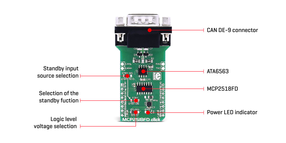
The Click board™ consists of a transceiver IC, a low-level physical layer IC (PHY) which provides a physical connection with the CAN bus itself, and a CAN controller IC, which is used as an interface between the MCU and the PHY IC. MCP2518FD click uses the ATA6563, a high-speed CAN transceiver with Standby mode, and the MCP2518FD, CAN FD controller with the SPI interface, both ICs by Microchip.
The role of the CAN bus controller is to provide arbitration, message framing, message validation, error detection, message filtering, and so on. Among all other tasks - it is used to provide clearly formatted CAN data for the application layer, running on the host MCU.
CAN Transreceiver
As the physical layer (PHY) IC, the ATA6563, a high-speed CAN transceiver with Standby mode, by Microchip. This IC provides the physical connection with the CAN bus and as such, it provides high resistance to electrostatic discharge and other electromagnetic phenomena, with its bus pins protected against transients, often encountered in the automotive environment. It allows communication speed up to 5Mbps. For the CAN bus device, it is important not to block the entire bus by permanently setting itself as the dominant node. For this reason, the PHY IC has the TX time-out function. It is also important to have defined bus pin states of nodes at all times. The ATA6563 PHY IC has its functional behavior predictive under all supply conditions. The ATA6563 is powered directly from the mikroBUS™ 5V power rail. This IC can work in several modes:
Normal mode is engaged when the STBY pin is at the logic LOW level, while the TXD pin is held to a HIGH logic level. While in the Normal mode, bus biasing is set to half the supply voltage, and the data can be transmitted and received via the CANH and CANL bus lines.
If the STBY pin of the ATA6563 is set to a HIGH logic level, the PHY IC will enter the Standby mode. While in Standby mode, the device is not able to transmit or correctly receive any data. The internal TX and HSC (high-speed comparator) sections are turned off, reducing the power consumption. Also, the bus lines are biased to the GND level. While in Standby mode, the device actively listens to the CAN bus traffic, looking for a valid wake-up pattern.
Since the STBY pin directly controls the operating mode of the PHY IC, it is routed to the onboard SMD jumper labeled as the STBY, allowing more than one way of control. This SMD jumper allows choice between connecting the STBY pin to the GND directly (LOW logic level), or allowing it to be controlled via the source selected by yet another SMD jumper, labeled as STBY SEL: control via the AN pin of the mikroBUS™, or the INT0/GPIO pin of the CAN control module IC.
CAN BUS controller
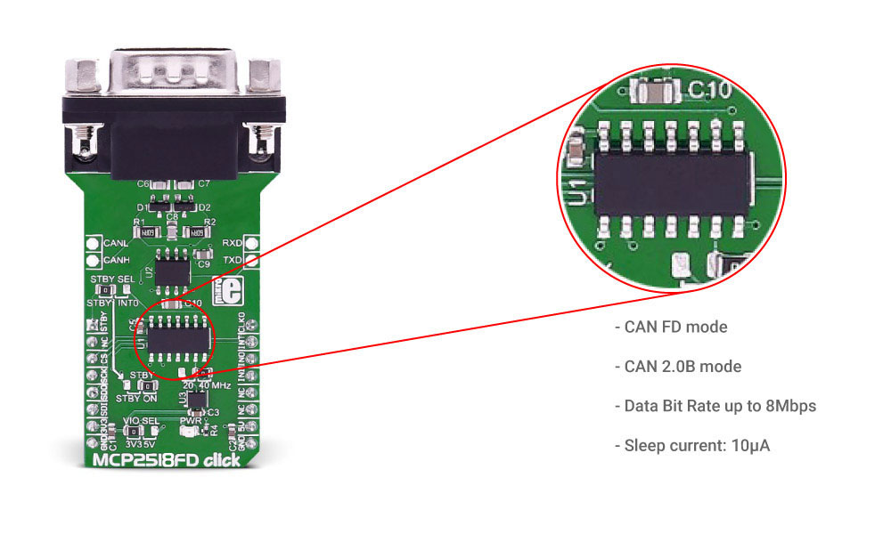
The MCP2518FD, CAN FD controller with the SPI interface, also by Microchip, is used to control and shape the CAN bus data traffic. While the PHY IC provides CAN communication on a basic - physical level, the MCP2518FD takes care of all the communication and data formatting. It manages the proper decoding and encoding of messages, data arbitration, message transmission prioritizing and filtering, provides the FIFO buffer for the messages, and so on. This IC can even provide a clock source to the host MCU, reducing the number of needed components to a minimum. On one end, it uses the SPI to communicate with the host MCU, while on the other end, it uses RXCAN and TXCAN pins to communicate with the PHY layer IC. The MCP2518FD supports CAN frames in classic format (CAN2.0B), as well as the CAN Flexible Data Rate format (CAN FD), as specified in ISO11898-1:2015.
CAN FD controller IC contains 2K of integrated RAM, which is used as the message buffer. Besides this, it also contains a number of SFR registers, used to configure and operate the controller IC, including the configuration of the INT/GPIO pins, their direction and polarity, configuration of the clock section, operating mode (including the Low Power mode for the MCP2518FD IC), FIFO control and message filtering, and so on. All the registers are 32bit wide. The datasheet of the MCP2518FD IC can be consulted for a comprehensive list of all the SFR registers and their functions. However, the provided library contains functions which can be used with MikroElektronika compilers. The included example application demonstrates the use of these functions, and it can be used as a reference for custom development.
There are three interrupt pins routed to the mikroBUS™: INT, INT0, and INT1, pins of the MCP2518FD IC are routed to the INT, TX and RX pins, respectively. While the INT pin is always an interrupt output pin, used to alert the MCU of the interrupt event that is enabled and has its flag bit activated, INT0 and INT1 pins are used to alert the MCU about the RX and TX events (if these interrupts are enabled), or as the GPIO pins. INT0 pin is also routed to the onboard SMD jumper labeled as STBY SEL, so that can be used to control the PHY IC standby mode. All interrupt pins are active low.
CLKO pin from the MCP2518FD IC is routed to the PWM pin of the mikroBUS™. This pin can be used to provide the clock output for the host MCU. Before it is used, it has to be configured via the SFR registers. It is derived from the input clock, generated by the onboard chip oscillator. The onboard SMD jumper allows frequency selection between 20MHz and 40MHz.
This IC can be interfaced directly to the MCU pins. To provide support for both the 3.3V and 5V operating MCUs, the Click board™ is provided with the onboard SMD jumper. This jumper determines only the logic voltage level and it is routed to both the VCC pin of the MCP2518FD IC and the VIO pin of the ATA6563. However, for proper operation of the Click board™, both 3.3V and 5V rails from the mikroBUS™ are used.
The Click board™ comes equipped with the standard DB-9 connector, making the interfacing with the CAN bus simple and effortless.
Specifications
| Type | CAN |
| Applications | It can be used for developing reliable custom CAN applications by using a wide range of MCUs, even if the used MCU does not include an integrated CAN module. |
| On-board modules | MCP2518FD, CAN FD controller with the SPI interface from Microchip; ATA6563, high speed CAN transceiver with Standby mode, from Microchip |
| Key Features | Expands the existing MCU with the reliable and robust CAN connectivity option. Support for both CAN 2.0B and CAN FD frames, high speed CAN communication up to 5 Mbps, integrated DB9 connector... |
| Interface | GPIO,SPI |
| Input Voltage | 3.3V,5V |
| Click board size | M (42.9 x 25.4 mm) |
Pinout Diagram
This table shows how the pinout on MCP2518FD click corresponds to the pinout on the mikroBUS™ socket (the latter shown in the two middle columns).
| Notes | Pin | Pin | Notes | ||||
|---|---|---|---|---|---|---|---|
| Standby control IP | STBY | 1 | AN | PWM | 16 | CLKO | Clock OP |
| NC | 2 | RST | INT | 15 | INT | Interrupt OP | |
| Chip select | CS | 3 | CS | TX | 14 | INT0 | Int/GPIO 0 / ATA6563 StdBy |
| SPI Clock | SCK | 4 | SCK | RX | 13 | INT1 | Int/GPIO 1 |
| SPI data OP | MISO | 5 | MISO | SCL | 12 | NC | |
| SPI data IP | MOSI | 6 | MOSI | SDA | 11 | NC | |
| Power supply | +3.3V | 7 | 3.3V | 5V | 10 | +5V | Power supply |
| Ground | GND | 8 | GND | GND | 9 | GND | Ground |
Additional Pins
| Name | I/O | Description |
|---|---|---|
| TX_CAN | I | CAN transmit |
| RX_CAN | O | CAN receive |
| CANL | I/O | CAN low line |
| CANH | I/O | CAN high line |
Jumpers And Settings
| Designator | Name | Default Position | Description |
|---|---|---|---|
| JP1 | VIO.SEL. | Left | Logic level voltage selection: left position 3V3, right position 5V |
| JP2 | STBY | Right | Selection of the Standby function: left position - ON, right position - STBY SEL configuration |
| JP3 | STBY SEL | Left | STBY input source selection: left position - STBY pin, right position - mikroBUS™ INT0 pin |
| JP4 | 20/40MHz | Right | Clock frequency selection: left position - 20MHz, right position - 40MHz |
LEDs And Buttons
| Designator | Name | Type | Description |
|---|---|---|---|
| CN1 | - | CONNECTOR | DB9 connector for CAN |
Software Support
We provide a library for the MCP2518FD Click on our LibStock page, as well as a demo application (example), developed using MikroElektronika compilers. The demo can run on all the main MikroElektronika development boards.
Library Description
Library offers a choice to exchange messages with the other device by using CAN communication. Library also offers a choice to access a control, status and RAM registers of the device. For more details check documentation.
Key functions:
void MCP2518FD_transmitMessage( uint8_t numDataBytes, uint8_t *transmitFlag, uint8_t *dataIn )- Transmits the desired message and checks is message successfully sent.void MCP2518FD_receiveMessage( uint8_t *receiveFlag, uint8_t *dataOut )- Receives the message and checks is message successfully received.int8_t MCP2518FD_Configure(T_MCP2518FD_id index, T_MCP2518FD_cfg* config)- CAN Control register configuration.int8_t MCP2518FD_ConfigureObjectReset(T_MCP2518FD_cfg* config)- Reset Configure object to reset values.
Examples description
The application is composed of the three sections :
- System Initialization - Initializes peripherals and pins.
- Application Initialization - Initializes SPI interface and performs the device configuration to work properly.
- Application Task - (code snippet) - Always checks is new message in FIFO ready for receiving and when is message ready, receives a message from the other device. Also in this example we can sent the desired message via CAN communication to the other device. We can choose a message to be sent by sending the determined command to the UART. In this example the command, which determines a message, can be number from 1 to 7.
void applicationTask()
{
    if (UART_Rdy_Ptr())
    {
        rxDat = UART_Rd_Ptr();
        chPtr = &txd[0];

        switch (rxDat)
        {
            case '1' :
            {
                _strcpy( chPtr, &txtMessage1[0] );
                MCP2518FD_transmitMessage( 5, &checkFlag, &txd[0] );
                if (checkFlag == 1)
                {
                    mikrobus_logWrite( "Message Sent", _LOG_LINE );
                }
            break;
            }
            case '2' :
            {
                _strcpy( chPtr, &txtMessage2[0] );
                MCP2518FD_transmitMessage( 7, &checkFlag, &txd[0] );
                if (checkFlag == 1)
                {
                    mikrobus_logWrite( "Message Sent", _LOG_LINE );
                }
            break;
            }
            case '3' :
            {
                _strcpy( chPtr, &txtMessage3[0] );
                MCP2518FD_transmitMessage( 2, &checkFlag, &txd[0] );
                if (checkFlag == 1)
                {
                    mikrobus_logWrite( "Message Sent", _LOG_LINE );
                }
            break;
            }
            case '4' :
            {
                _strcpy( chPtr, &txtMessage4[0] );
                MCP2518FD_transmitMessage( 4, &checkFlag, &txd[0] );
                if (checkFlag == 1)
                {
                    mikrobus_logWrite( "Message Sent", _LOG_LINE );
                }
            break;
            }
            case '5' :
            {
                _strcpy( chPtr, &txtMessage5[0] );
                MCP2518FD_transmitMessage( 3, &checkFlag, &txd[0] );
                if (checkFlag == 1)
                {
                    mikrobus_logWrite( "Message Sent", _LOG_LINE );
                }
            break;
            }
            case '6' :
            {
                _strcpy( chPtr, &txtMessage6[0] );
                MCP2518FD_transmitMessage( 3, &checkFlag, &txd[0] );
                if (checkFlag == 1)
                {
                    mikrobus_logWrite( "Message Sent", _LOG_LINE );
                }
            break;
            }
            case '7' :
            {
                _strcpy( chPtr, &txtMessage7[0] );
                MCP2518FD_transmitMessage( 7, &checkFlag, &txd[0] );
                if (checkFlag == 1)
                {
                    mikrobus_logWrite( "Message Sent", _LOG_LINE );
                }
            break;
            }
            default :
            {
            break;
            }
        }
    }

    MCP2518FD_receiveMessage( &checkFlag, &rxd[0] );
    if (checkFlag == 1)
    {
        chPtr = &rxd[0];
        mikrobus_logWrite( "Received Message : ", _LOG_TEXT );
        mikrobus_logWrite( chPtr, _LOG_LINE );
    }
}
Additional Functions :
- char * _strcpy( char * _to, char * _from ) - String copy function.
The full application code, and ready to use projects can be found on our LibStock page.
Other mikroE Libraries used in the example:
SPIUART
Additional notes and informations
Depending on the development board you are using, you may need USB UART click, USB UART 2 click or RS232 click to connect to your PC, for development systems with no UART to USB interface available on the board. The terminal available in all MikroElektronika compilers, or any other terminal application of your choice, can be used to read the message.
MIKROSDK
This click board is supported with mikroSDK - MikroElektronika Software Development Kit. To ensure proper operation of mikroSDK compliant click board demo applications, mikroSDK should be downloaded from the LibStock and installed for the compiler you are using.
For more information about mikroSDK, visit the official page.
Downloads
mikroBUS™ Standard specification
Write a review
Your Name:
Your Review:
Note: HTML is not translated!
Rating:
Bad
Good
Enter the code in the box below:
-
 ₹1,889.00


© 2026, MG Automation Technologies. Powered by MG Super LABS.Find us on Google+
Designed with by Ish Gupta